✏️ Explanatory Question
[Computer Hardware]
Question:
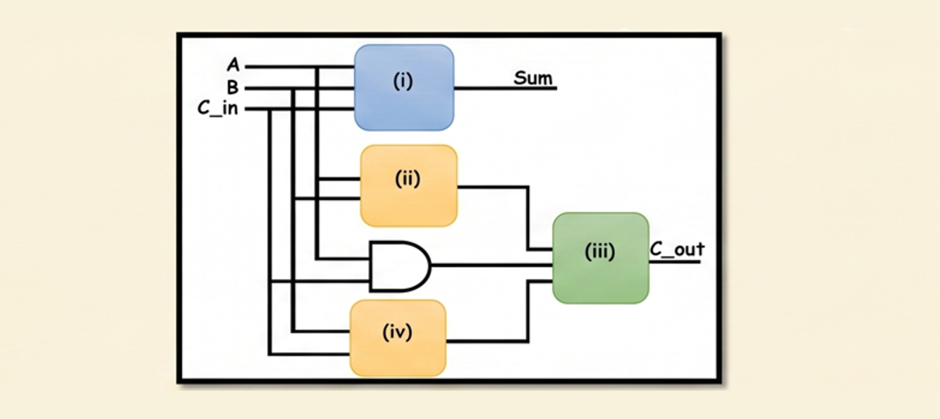
Following is the circuit diagram of a Full Adder. Redraw the circuit diagram by adding the missing logic gates.
[Computer Hardware]
Question:
Following is the circuit diagram of a Full Adder. Redraw the circuit diagram by adding the missing logic gates.
Answer:
The missing logic gates are:
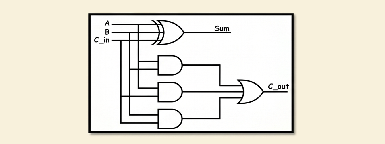
(i)  XOR Gate
(ii) AND Gate
(iii) OR Gate
(iv) AND Gate
Explanation:
A Full Adder has:
A, B, C_inSum, C_outSum Expression:
Sum = A ⊕ B ⊕ C_inTherefore, gate (i) must be:
XOR GateCarry Output Expression:
C_out = AB + BC_in + AC_inCarry output is produced using:
Hence:
(ii) → AND Gate
(iv) → AND Gate
(iii) → OR Gate
Conclusion: